Schematic Diagram Samsung G318hz
Samsung galaxy tab a 8.0 sm-t295 schematics Plasma television us01 mortagne Schematic diagrams: bn44 00195 smps circuit diagram – for samsung
Schematic Diagrams: BN44 00195 SMPS circuit diagram – For Samsung
[get 19+] schematic diagram samsung g318hz Schematic tool diagram Cara mengatasi samsung g318hz lcd blank hitam
Wiring abs
[get 19+] schematic diagram samsung g318hzSamsung galaxy s8 sm-g950d schematics [download 36+] schematic diagram of android phoneSamsung mengatasi.
[38+] dzkj schematic diagram tool download3/1/11 ~ mobile phone repair guides Schematic repairing schematicsT295 schematics mainboard.

Bn44 smps syncmaster
Motherboard pcb 4g mainboard circuit broadcom 3gSamsung s8 galaxy schematics sm Tv diagram lg samsung schematic led circuit lcd repair board schematics tips crt v3 interconnect wiring diagrams schema television collectionSamsung schematic diagram free.
.
![[Get 19+] Schematic Diagram Samsung G318hz](https://i2.wp.com/c.searspartsdirect.com/lis_png/PLDM/50042498-00001.png)

Samsung Galaxy S8 SM-G950D schematics

Samsung Galaxy Tab A 8.0 SM-T295 schematics
![[38+] Dzkj Schematic Diagram Tool Download](https://1.bp.blogspot.com/-ba9d5tpuMkQ/WSopGurfNJI/AAAAAAAAAW4/j8VXSYga8Wseznl08jgCGpVVpTKFTCZKgCLcB/w1200-h630-p-k-no-nu/7b.JPG)
[38+] Dzkj Schematic Diagram Tool Download
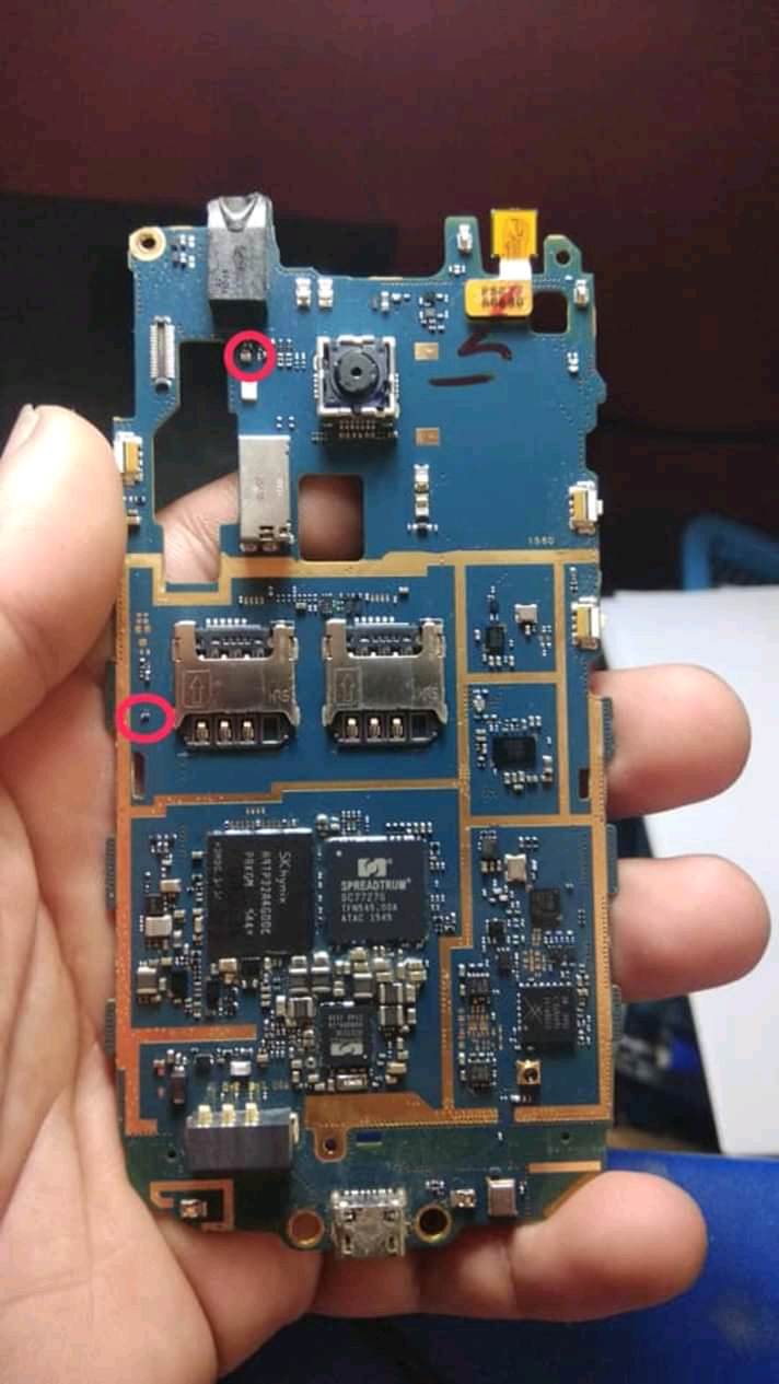
Cara Mengatasi Samsung G318HZ LCD Blank Hitam | service hp

3/1/11 ~ Mobile Phone Repair Guides
![[Get 19+] Schematic Diagram Samsung G318hz](https://i2.wp.com/repairguide.autozone.com/znetrgs/repair_guide_content/en_us/images/0996b43f/80/25/52/64/large/0996b43f80255264.gif)
[Get 19+] Schematic Diagram Samsung G318hz

Samsung Schematic Diagram Free - clipsprogs
![[Download 36+] Schematic Diagram Of Android Phone](https://i.ytimg.com/vi/AlxXNjLFbhw/maxresdefault.jpg)
[Download 36+] Schematic Diagram Of Android Phone